Making a custom PCB ornament
I decided this year to make an ornament for our tree. The timing coincided with a creative itch and a business need to actually go through the process of printed circuit board (PCB) design and manufacturing, so I thought I’d make a little tree gadget.
And I’m really happy with the results!
This is my first custom circuit board and it actually worked the first time! I’ll walk you through the process so that you can see what this involves. Many of the concepts and jargon were new to me, so hopefully this serves as an orientation for you if you’re about at the stage that I am — or if you’re just curious.
Operation & choosing the “brain”
When you push the button, the circuit powers up (or comes out of sleep mode; more on this later) and then plays a snippet from “Jingle Bells” while lighting the tree-topper yellow light and alternating the green and red lights on and off. After the song finishes, it waits for a few seconds, then starts all over until you press the button again to put it to (power saving) sleep.
A few months ago, I acquired an ATtiny25 microcontroller, which are typically available for about $1 US. The ATtiny85 seems to be more popular as it features 8KB of program space and 512B (yes, bytes) of RAM. The ATtiny25 only has 2KB of program space and 128B of RAM, but that’s (just) enough for a simple application like this.
Sketch uses 1940 bytes (94%) of program storage space. Maximum is 2048 bytes.
Global variables use 92 bytes (71%) of dynamic memory, leaving 36 bytes for local variables. Maximum is 128 bytes.
I’ve also wanted for a while to experiment with bare chips like the ATTiny rather than something that already has an FTDI USB bridging chip to plug into your computer. I’ve played with a PICAXE once or twice (in BASIC!) which was fun, but I just decided to go ATtiny to try something new since I’d heard so much about the ATtiny85 in projects. As documented on a number of places on the web, you can use an Arduino Uno as a programmer to bridge the gap between writing the code on your computer and uploading it to the chip.
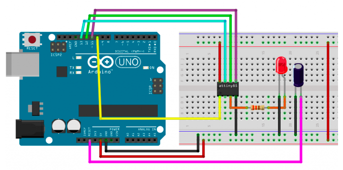
One fun tidbit here is that in my programmer circuit (unlike the above), I had the lights and beeper hooked up on the same lines as the data read & write from the Arduino, so whenever I would send the code over, I’d get rapid-fire clicking noises and a light show as the data was transferred.
I also found an amazing site by David Johnson-Davies with lots of fun little projects and experiments for the ATtiny chips. The ones I was able to make the most use of were his post on low power mode and one on push button on/off switches. These really helped with a design that could technically always remain ready but more or less shut itself off (by way of a sleep mode) yet still have the battery last a long time. He’s got a couple other incredible projects like this tiny MIDI player and others which use Direct Digital Synthesis to make more than beeps and boops and which completely blow my mind, so stay tuned (ha!) for a future project which I will certainly make along those lines.
Circuit design & prototyping
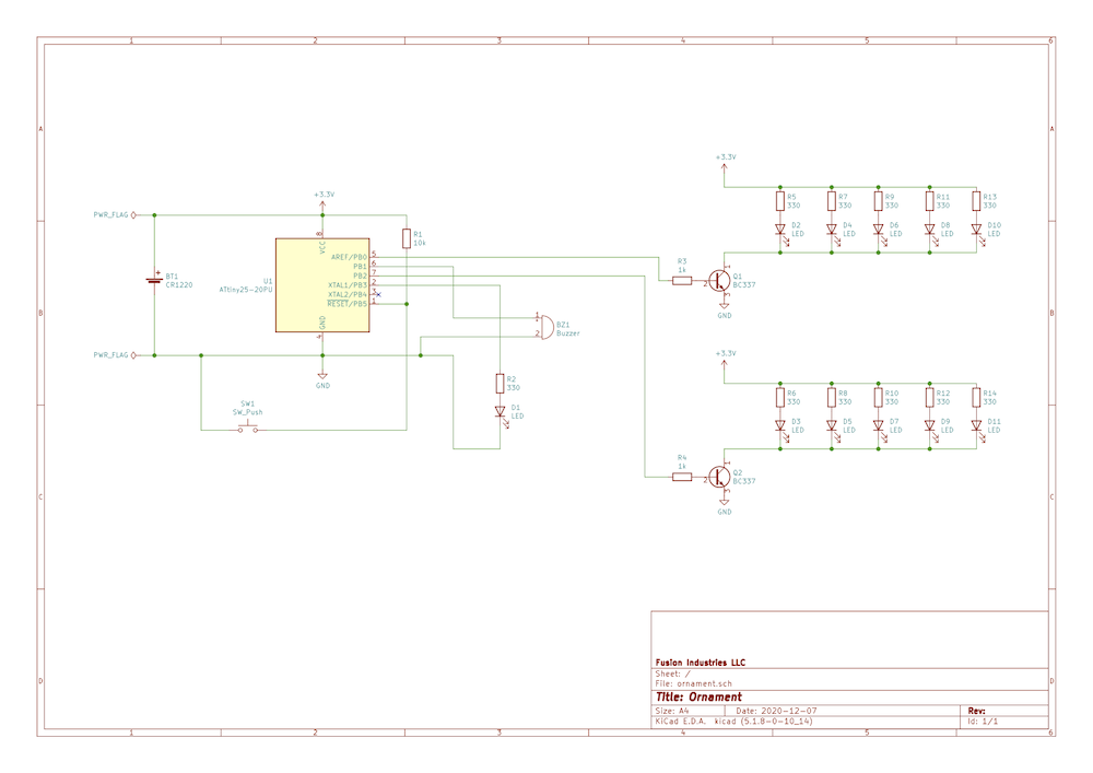
Here’s the final circuit schematic, which I made with KiCad, a free and open source tool:
This isn’t my first schematic with KiCad; more like fifth or sixth. But it’s the first one I continued on to the circuit board step.
The actual prototyping process is a mix of playing with stuff on a breadboard and drawing the schematic — don’t let the completed design fool you. When I got the first cut of things working, it basically looked like this:
In this first iteration, besides only having one light of each color, I flashed them in time to the music, which was a little brash. I also didn’t have a button, a solid yellow light, or battery power.
In the final circuit, one pin on the chip is power, one is ground, and a third is the reset. Then, for data, one pin drives the yellow light, one drives the beeper, and the sixth and seventh pins drive the red and green circuits by way of a transistor each to get power directly from the battery as five lights each would require too much current to drive off of a chip pin directly. The eighth and last pin on the chip is unused. Each LED has a current-limiting resistor, plus there is a reset pin pullup on the switch circuit and two more for the transistor bases. The bill of materials comes in at under $10 US for the components — which would be far less for things like resistors bought in bulk. And making a BOM was a first for me, too!
I ended up using ATTinyCore in order to get access to the Arduino standard library tone() function rather than use one of David’s musical approaches, mostly out of simplicity and ease of code legibility and debugging.
The next step was to prototype the full circuit, especially if I was going to spend money to get a board made. I wanted to make sure that this exact circuit worked. And it did! The only thing different below was that I had a master power switch close to the battery while I was testing low-power sleep mode so that I didn’t accidentally run down the battery. At this step, I moved to a timer-based approach so that I could flash the lights at a constant rate unrelated to the music.
By the way, I got the sheet music for Jingle Bells here and just transcribed the musical notes to frequencies using this reference.

Fortunately, I can read music.
The final Arduino code listing looks like this:
// power routine based on http://www.technoblogy.com/show?VOO
// tone on ATtiny25 via https://github.com/SpenceKonde/ATTinyCore

#include <avr/sleep.h>

int Power __attribute__ ((section (".noinit")));

const uint16_t scale[] = {
  262,294,330,349,392
};
const uint8_t n[] = {
  2,2,2,2,2,2,2,4,0,1,2,
  3,3,3,3,3,2,2,2,2,4,4,3,1,0
};
const uint8_t ds[] = {
  5,10,20,40
};
const uint8_t d[] = {
  1,1,2,1,1,2,1,1,1,1,3,1,
  1,1,1,1,1,1,0,0,1,1,1,1,3
};

const uint8_t red = 0;
const uint8_t beep = 1;
const uint8_t green = 2;
const uint8_t yellow = 3;
const uint8_t nc = 4;

int active = 0;
int timer = 0;

void PowerDown() {
  set_sleep_mode(SLEEP_MODE_PWR_DOWN);
  ADCSRA &= ~(1<<ADEN);
  sleep_enable();
  sleep_cpu();
}

void setup() {
  Power = !Power;
  if (!Power) PowerDown();
  pinMode(red, OUTPUT);
  pinMode(beep, OUTPUT);
  pinMode(green, OUTPUT);
  pinMode(yellow, OUTPUT);
  pinMode(nc, INPUT_PULLUP);
}

void loop() {
  digitalWrite(yellow, HIGH);
  timer = millis();
  for (int i=0; i<25; i++) {
    digitalWrite(active, HIGH);
    tone(beep, scale[n[i]]);
    unsigned long dur = (unsigned long)ds[d[i]] * (unsigned long)20;
    int frag = dur / 10;
    for (int j=0; j<dur; j=j+frag) {
      if (millis() > timer + 500) {
        digitalWrite(active, LOW);
        active = (active == red) ? green : red;
        digitalWrite(active, HIGH);
        timer = millis();
      }
      delay(frag);
    }
    noTone(beep);
    delay(100);
  }
  digitalWrite(red, LOW);
  digitalWrite(green, LOW);
  digitalWrite(yellow, LOW);
  delay(5000);
}
Not the most readable code, mostly because I had to save a little space to fit into the flash space & RAM. Of note is that all the frequencies used in the tune are in scale once, then the n array indicates which of those to play in order. The ds are possible base durations, in milliseconds (essentially, sixteenth, eighth, quarter, and half notes), then lastly, the d array references each of those to match the note order in n. This saved a little space over repetitively listing the frequencies and durations directly.
Per David’s recommendations, I set the unconnected chip pin nc to use the internal pull-up resistor in order to avoid floating and to use less power when sleeping.
Lastly, the dur and frag business is how I multiplied out the actual tempo that I wanted and how I check during the playing of a note (in this case, ten times during each note) if a half second has passed and if so, alternate the red and green lights.
Board layout
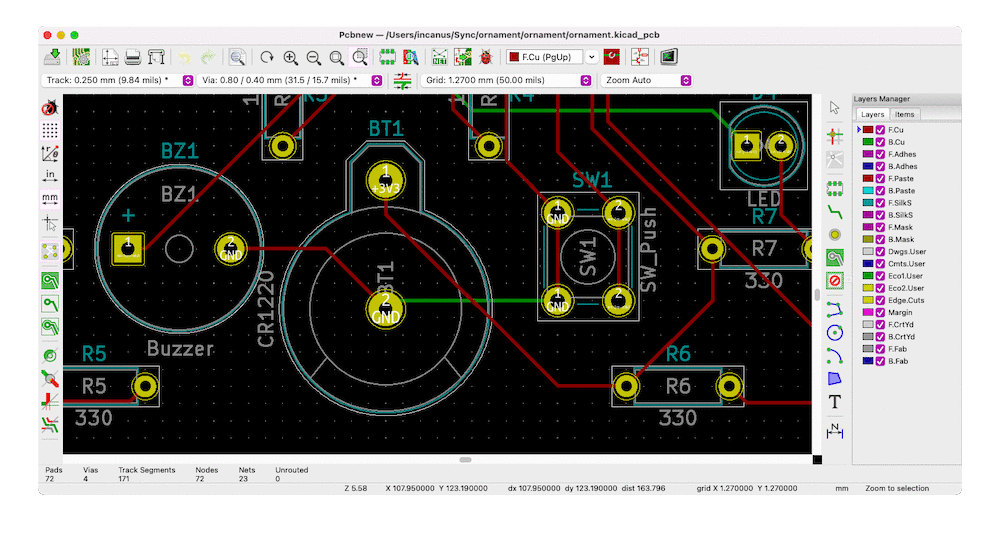
Once the design work was done, it was time to get the board laid out, which was the biggest learning chunk of the project.
There’s not a lot to say about it other than that you have to think in three dimensions, try to keep bends in traces at 45-degree rather than 90-degree angles to avoid interference (though it doesn’t matter as much in a simple circuit like this), and make things look nice, if possible. Again, this was in KiCad. I highly recommend just playing around as well as following their documentation tutorials. It just takes time.
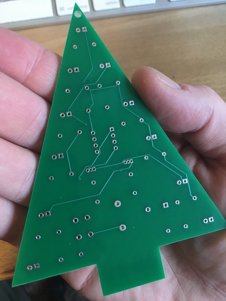
The only major roadblock I had was that since I wanted to use a two-layer board (not four or more) both for lower cost as well as lower complexity, originally I was going to use the second, back layer for a ground plane and connect all grounds to it as a convenience. But it quickly became apparent that it would be impossible to avoid crossing wires on the front side (which wouldn’t function properly, if at all) since I brilliantly decided to zigzag the connected lights of a same color back and forth across the board. Eventually, I realized that the grounds could all just run back to the battery and then I could work in true three dimensions and allow the traces to jump from front to back as needed to avoid intersecting.
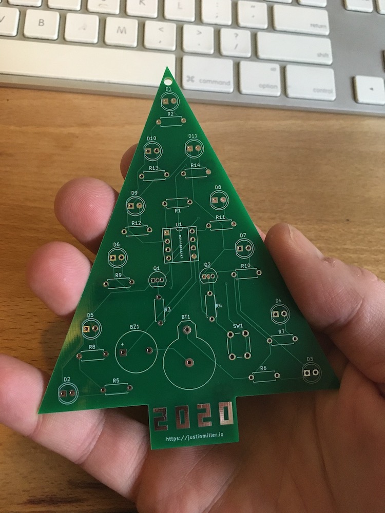
The completed board design looks something like this:
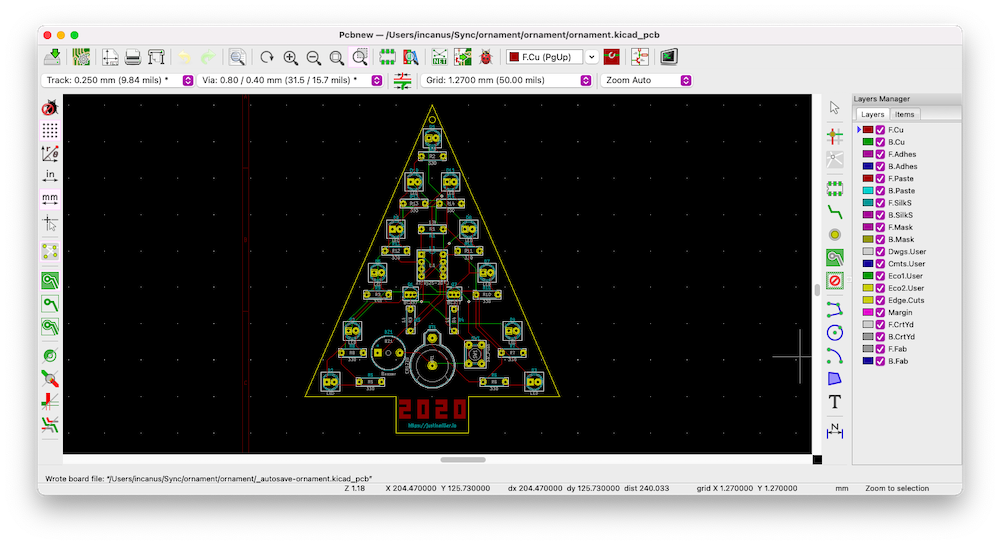
You essentially get the silkscreened parts, both labels and outlines, for free when you assign “footprints” for each of your schematic components based on their real-world hardware. You just move them into place (which I did, aiming for symmetry). All the red and green traces (how appropriate!) were laid down manually, and I either made use of component holes to bridge between front and back or, in three cases, created manual “vias”, which were isolated holes, to do so. Here you can see all three — look for the white holes that are not part of a component footprint and where the traces switch from red (front) to green (back) in the middle of nowhere.
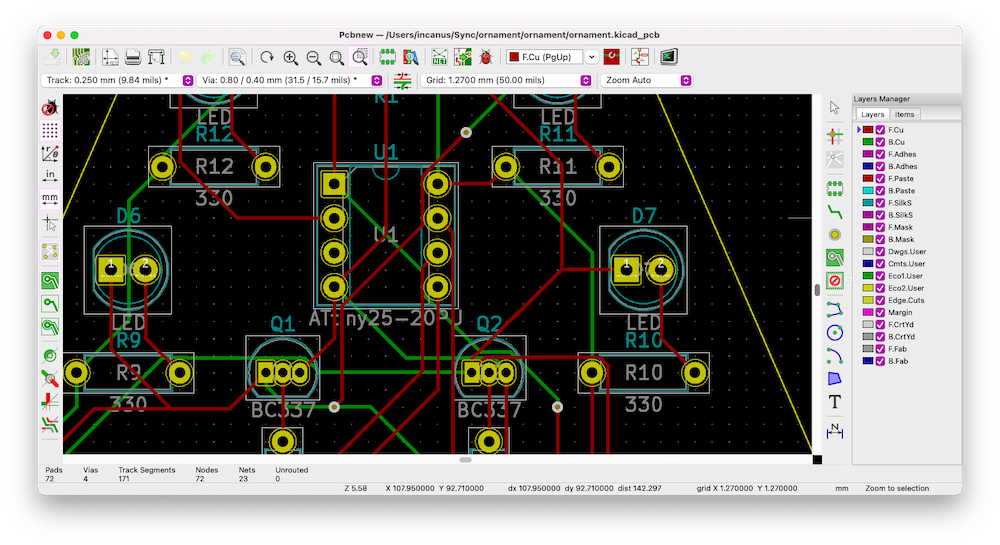
Sometimes, things get dense. Fortunately, you can toggle on and off all of the layers, so that you can start to do things like just look at the traces that you are laying down.
It’s also a vector-based drawing tool, so things zoom and render nicely even at high levels.
Eventually, things were wrapped up and the rules engine showed no disconnected components or other problems.
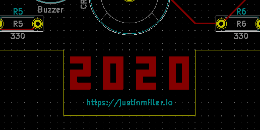
Two last touches that I added were a silkscreen of my website address and, after a little puzzling and finding this Reddit post, an electrically-inactive bare copper date for a little flair.
Amazingly, KiCad even has a 3D viewer option!
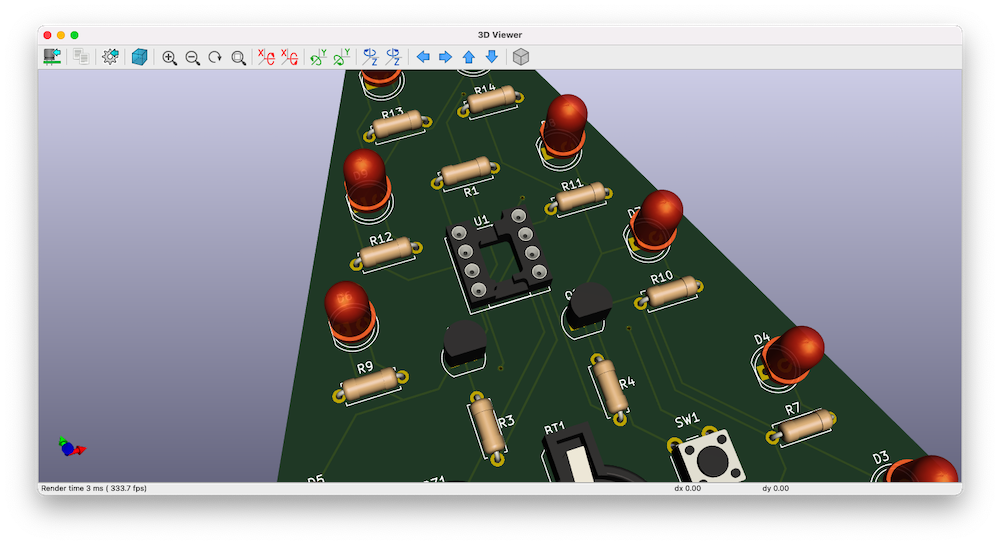
While it’s not trivial to have differently-colored LEDs in this view, I wasn’t too worried about that. I knew from my schematic layout and the BOM that D1 was yellow, then the evens D2-D10 were red and odds D3-D11 were green.
Vendor selection & Gerber upload
The industry uses a set of file formats called “Gerbers” which is what manufacturers expect. In my case, I decided to try PCBWay for my first ever boards. On principle, I actually wanted to go with the local Oshpark, but a combination of time crunch and ease of use (particularly this guide on generating Gerbers from KiCad) had me go with PCBWay. I was able to zip everything together and upload it to their control panel, tweak a few settings like choosing a green board (naturally!) and my order was on its way. I uploaded things on the evening of December 9 in my time zone and they shipped from the factory in China on December 11.
Not counting a little rush shipping, it was $32 US for (the minimum order of) five boards. This could be done cheaper (by a lot, especially in quantity — as cheap as $2.50 US in some cases, if not cheaper), but I was in a hurry, unsure of the success of the design, and I felt that this was a fair price for the learning experience.
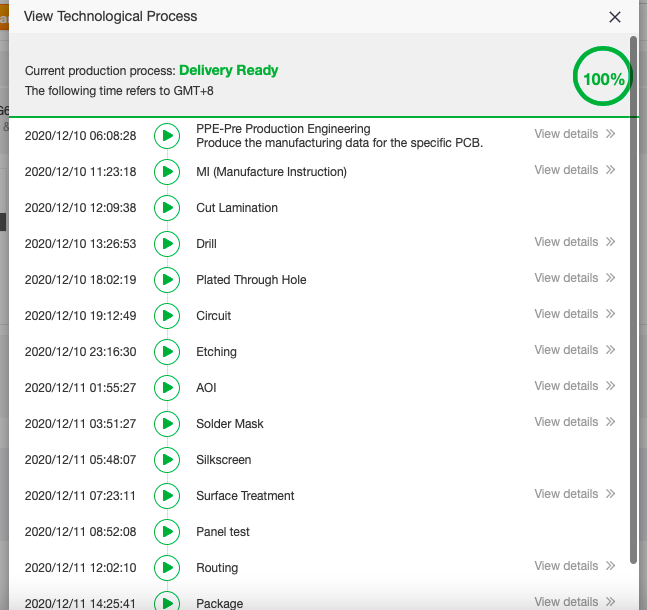
And PCBWay’s process tracking is amazing! This was all available in realtime.
Delivery & assembly
I got the boards in the early afternoon on December 15, less than a week after I finished the design and uploaded it to China. Amazing. And the boards looked great!
They also of course checked out technically — I tested each with a multimeter.
Each one took about a half-hour to solder up, which I did by placing all of the components through the holes, soldering, snipping off the leads, and cleaning things up. I made all five ornaments successfully.
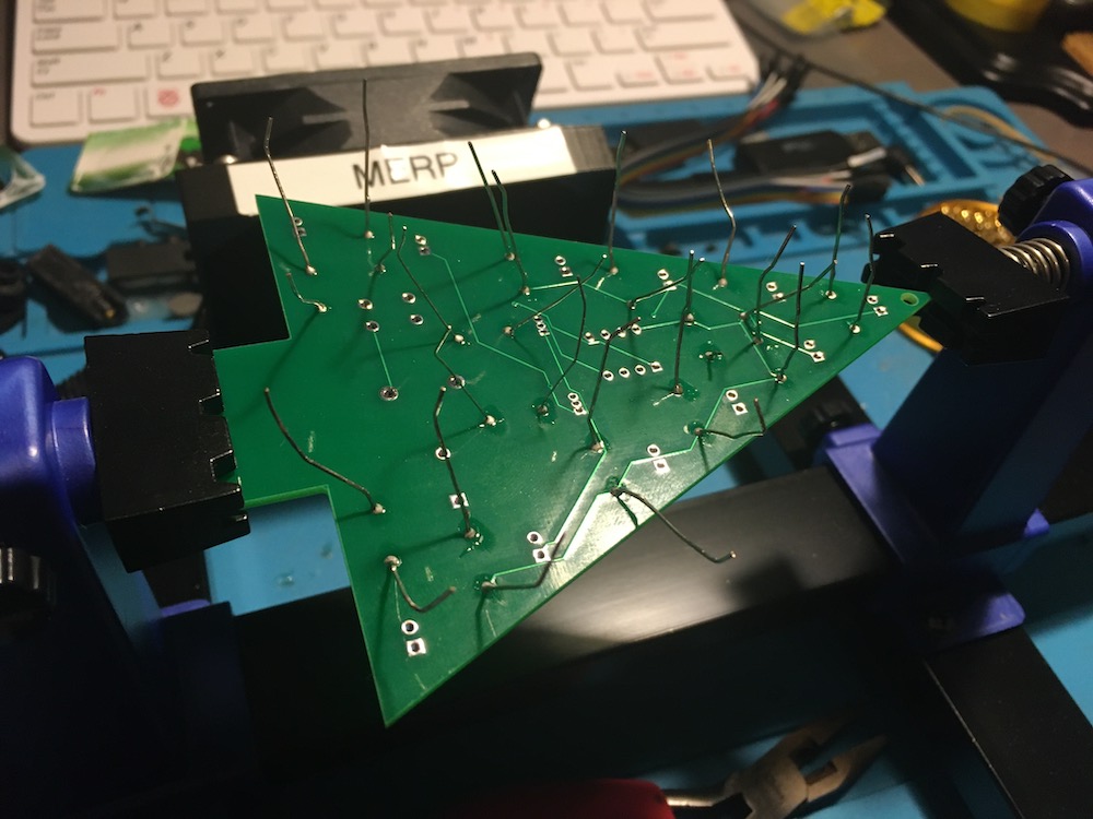
One thing that would do over is to use or make a transistor footprint with the holes a little further apart and bend the transistors to fit. This would allow for a little more space when soldering — things got very tight!
Another tip (or best practice, maybe) that I would pass along are to use sockets for the chips, for two reasons: it’s safer for the chip with regard to heat while soldering, and the chip can be replaced or reprogrammed easily. I did a mix of sockets and chips directly on the board — once I was able to test each chip after programming in a socketed board, I felt comfortable soldering some chips directly to a board.
Conclusion
This project was an amazing learning experience and I came away incredibly impressed by the service that PCBWay offers. When people speak of China’s manufacturing superiority and cost-effectiveness, this is what they’re talking about. For future projects, however, I’d love to explore domestic options and I’ll try to report back about what I learn.
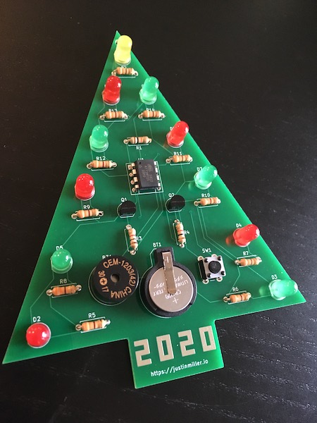
Again, here’s the final result (see the top of the post again for the video):
Next year, I’m hoping to get started earlier, make many more boards, perhaps have them assembled as a service, and make them available to others, assembled or as a kit!
Happy Holidays!
🎄